ANN regression with a VAE structure · 2023
AMS Circuit Design Optimization Technique Based on ANN Regression Model with VAE Structure (opens in a new tab)
IEEE ACCESS (vol. 11, pp. 58850-58862)
Funding IITP-2023-RS-2022-00156295
Publication details
RESEARCH · AI & DESIGN AUTOMATION
Learning-based optimization for analog and mixed-signal circuits, from transistor-level design to RF passive components.
THE SHARED IDEA
Design automation turns repeated circuit sizing and layout exploration into a data-guided search. Designers define the parameters and performance targets, build training data with SPICE or electromagnetic (EM) simulation, and train neural networks to predict how new designs will behave. This makes it practical to compare many candidates while concentrating simulation effort on promising designs. The two studies apply this idea to transistor-level AMS optimization with a VAE-style model and PCELL-based RF inductor optimization, helping designers navigate competing goals such as jitter, power, inductance, quality factor, and area. Simulation remains the physical reference for judging candidate designs.
Transistor dimensions or inductor geometry
SPICE or EM data pairs designs with performance
An ANN predicts performance for new designs
Compare candidates against the design targets
Check promising designs with physical simulation
01 / ANN REGRESSION & VAE
An artificial neural network (ANN) regressor learns a numerical mapping from paired inputs and outputs. Hidden layers combine the inputs through adjustable weights and nonlinear functions. Training reduces the difference between predicted and simulated values; the trained network can then evaluate new parameter combinations.
The inputs are design choices, and the outputs are predicted performance values, such as delay or power. Multiple outputs let one model describe several performance quantities together.
| Model element | Ring-VCO example in the paper |
|---|---|
| Inputs | Channel width/length (W/L), PMOS/NMOS width ratio, and control voltage. |
| SPICE targets | RMS jitter, average period, duty cycle, power, rising time, and falling time. |
| Selection | Jitter–power FoM, with frequency and duty-cycle filtering. |
The paper’s VAE-style structure pairs parameter-to-performance prediction with performance-to-parameter prediction. Decoding and noise propose distinct parameter sets with similar predicted behavior. These candidates enter SPICE verification before fine optimization.
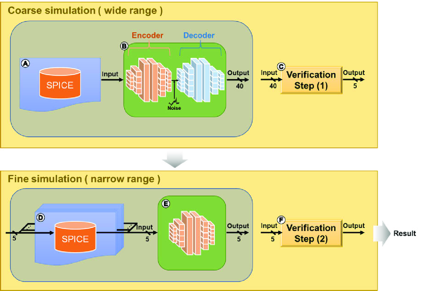
SPICE samples span the full parameter range.
Forward and reverse models expand ten candidates to at most forty.
Rank by FoM, test slow-slow (SS) and fast-fast (FF) corners, and retain five candidates.
Resimulate candidate neighborhoods; window size follows prediction error.
Train a forward model for each narrowed design region.
Compare FoM sensitivity under parameter perturbations and select the final design.
A nominal optimum may be sensitive to small parameter changes. Verification therefore considers stability alongside performance. The study evaluates ring-VCO designs in 180 nm, 65 nm, and 45 nm CMOS.
02 / RF PASSIVE DESIGN
A parameterized cell (PCELL) generates a layout from numerical settings. The paper varies inner radius, turn count, metal width, spacing, asymmetry ratio, and polygon side count. These settings change the conductor path and its electromagnetic behavior. Figure 2 shows how the geometry is constructed, including stepped diagonal routing that accommodates the process routing rules.
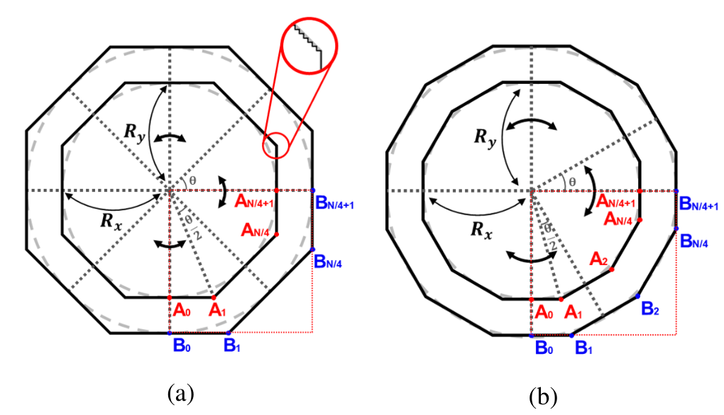
Inductance L describes the reactive response, while quality factor Q compares reactance with loss. Geometry affects both inductance and losses, so the design must satisfy the required L and Q at the operating frequency while fitting the available area.
The ISOCC study combines PCELL generation with an ANN trained on electromagnetic (EM) simulation data. It supports polygonal, circular, and asymmetric layouts in 65 nm CMOS with one polysilicon and nine metal layers (1P9M). Initial sampling and training are performed for each topology; the learned model then interpolates the design space. Candidate selection considers inductance, operating frequency, area, tolerance, and self-resonant frequency, followed by EM verification of the selected design.
Vary geometry settings through the PCELL rather than drawing each candidate separately.
Associate each simulated geometry with its EM-derived electrical behavior.
Learn geometry-to-performance relationships with ANN regression.
Select a candidate within the design constraints, then check it with EM simulation.
CIRCUITS & PASSIVE COMPONENTS
Our research uses learned models to explore design choices efficiently while keeping circuit and electromagnetic behavior central to the optimization.
| Focus | AMS optimization | Inductor automation |
|---|---|---|
| Design object | VCO circuit parameters | RF inductor geometry |
| Learning model | ANN with a VAE structure | ANN regression |
| Simulation foundation | SPICE and PVT characterization | EM characterization |
| Design objective | Performance and PVT sensitivity | Inductance, quality factor, and area |