ADC-based wireline reception · 2020
A 12.8-Gbaud ADC-based Wireline Receiver with Embedded IIR Equalizer
IEEE J. Solid-State Circuits, vol. 55, no. 3, pp. 557 - 567, Mar. 2020.
Publication details
RESEARCH · SENSOR INTERFACES & DATA CONVERTERS
Analog front ends, sensor readout circuits, and high-speed, low-power data converters for integrated ASIC systems.
01 / SIGNAL ACQUISITION & DIGITIZATION
A sensor produces an electrical signal that must be conditioned, converted, and processed before it becomes useful information. We design the analog front end and data converter together, balancing signal bandwidth, noise, conversion accuracy, and power consumption for the application.
Photodiode modeling, temperature sensing, and image-sensor readout connect physical signals with CMOS interface circuits. Circuit and layout choices determine how the signal is collected and prepared for digitization.
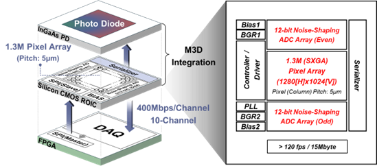
Our ADC research covers SAR, pipelined, flash, and sigma-delta architectures, including time interleaving, passive gain, and interpolation. The architecture and circuit implementation balance conversion speed, resolution, area, and energy.
Combining analog equalization with digitization supports high-speed wireline reception. Our published work includes an ADC-based receiver with embedded IIR equalization.